The videos and information in this post relate to an ECS Journal of Solid State Science and Technology focus issue called: Printable Functional Materials for Electronics and Energy Applications.
(Read/download the focus issue now. It’s entirely free.)
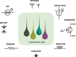
Printing technologies in an atmospheric environment offer the potential for low-cost and materials-efficient alternatives for manufacturing electronics and energy devices such as luminescent displays, thin-film transistors, sensors, thin-film photovoltaics, fuel cells, capacitors, and batteries. Significant progress has been made in the area of printable functional organic and inorganic materials including conductors, semiconductors, and dielectric and luminescent materials.
These new printable functional materials have and will continue to enable exciting advances in printed electronics and energy devices. Some examples are printed amorphous oxide semiconductors, organic conductors and semiconductors, inorganic semiconductor nanomaterials, silicon, chalcogenide semiconductors, ceramics, metals, intercalation compounds, and carbon-based materials.
A special focus issue of the ECS Journal of Solid State Science and Technology was created about the publication of state-of-the-art efforts that address a variety of approaches to printable functional materials and device. This focus issue, consisting of a total of 15 papers, includes both invited and contributed papers reflecting recent achievements in printable functional materials and devices.
The topics of these papers span several key ECS technical areas, including batteries, sensors, fuel cells, carbon nanostructures and devices, electronic and photonic devices, and display materials, devices, and processing. The overall collection of this focus issue covers an impressive scope from fundamental science and engineering of printing process, ink chemistry and ink conversion processes, printed devices, and characterizations to the future outlook for printable functional materials and devices.
The video below demonstrates Printed Metal Oxide Thin-Film Transistors by J. Gorecki, K. Eyerly, C.-H. Choi, and C.-H. Chang, School of Chemical, Biological and Environmental Engineering, Oregon State University.
Step-by-step explanation of the video:
Procedures for making printed Metal Oxide Thin-Film Transistors is demonstrated in this video.
Solution Preparation: Prepare metal halide precursor that is used as ink for printing.
Print Metal Halide Film with Inkjet Printer: Piezoelectric inkjet printer is used to manufacture the printed metal halide film.
Inject ink in the cartridge: Load 1-2 ml of precursor ink in the cartridge. Put a substrate on the printer station.
Select nozzels for printing: In order to get uniform film, it is important to select nozzles that shoot uniform ink droplets. Print Metal Halide Film with Inkjet Printer.
Annealing Process: The printed metal halide film is annealed to form metal oxide semiconductor.
Device Test with Probe Station: Measure electrical properties of TFT such as I-V curve, mobility, and on/off ratio by Probe Station.
The video below show demonstrates Inkjet Printed Conductive Tracks for Printed Electronic conducted by S.-P. Chen, H.-L. Chiu, P.-H. Wang, and Y.-C. Liao, Department of Chemical Engineering, National Taiwan University, No. 1 Sec. 4 Roosevelt Road, Taipei 10617, Taiwan.
Step-by-step explanation of the video:
For printed electronic devices, metal thin film patterns with great conductivities are required. Three major ways to produce inkjet-printed metal tracks will be shown in this video.
The most commonly-used one is silver nanoparticle ink. Typically, after ink loading, stable droplet ejection is needed for good printing quality. The printed silver tracks need to be sintered at a relatively high temperature for particles to fuse together, which can be observed from the color change after heating. The tracks can exhibit great conductivity close to that of bulk silver.
The second type is metal-organic decomposition. Well-printed ink patterns with great pattern fidelity can be formed by tuning print parameters like dot spacing. The printed silver salts are then transformed into silver after heated at 70 degree C for 10-20 minutes. Several tests, such as resistance measurements, bending and tape tests, are also performed to demonstrate the great conductivity, mechanical stability, and adhesion of printed silver tracks on flexible substrates.
The last demonstration is the inkjet reaction system. First, two inks are printed separately on the substrate. These two inks react and the so-called silver-mirror reation generate silver over the printed area at room temperature. After rinsing the printed thin film and dried at 70 degree C, the printed track shows good conductivity.
(Read/download the focus issue now. It’s entirely free.)
Acknowledgments
The authors would like to thank Mr. Kuan-Ming Huang and Mr. Chia-Wei Chang for their great help in recording and editing video clips.


