Your all-inclusive reservation at Moon Palace Resort includes unlimited meals, drinks, taxes and gratuities.
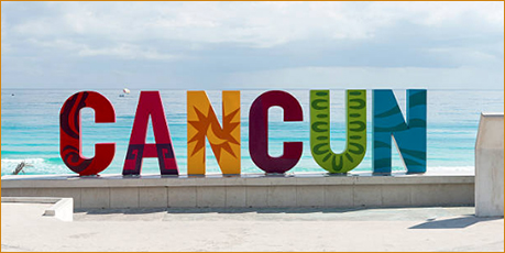
Join us for AiMES 2018, September 30 through October 4. This is a joint meeting with ECS and the la Sociedad Mexicana de Electroquímica being held at the Moon Palace Resort in Cancun, Mexico.
Moon Palace Resort is a gigantic all-inclusive luxury resort along Cancun’s Mayan Riviera amidst 55-acres of lush tropical foliage. Just minutes from the Cancun International Airport, it features a full-service spa and a 27-hole golf course designed by Jack Nicklaus, a larger-than-life pool, and countless restaurants and eateries making this resort truly all-inclusive.
The all-inclusive dining section includes all meals including breakfast, lunch, dinner, and unlimited snacks at any of the buffet style and a la carte restaurants, as well as beverages including alcohol. The Resort offers a variety of entertainment options for family members of every age and with different interests. There are non-stop activities including bicycling, basketball, beach volleyball, tennis, a teen’s lounge, a supervised kids club, a FlowRider to try your surfing skills, and mini-golf.
ECS has arranged a room block at the resort with rates starting at $364 per night.
Your all-inclusive reservation includes unlimited meals, drinks, taxes and gratuities.
Book Your Room Today!
Daily room rates include all of the following:
- All meals and drinks at the hotel including alcoholic beverages
- All hotel taxes and gratuities
- In-room wine, liquor dispenser, mini bar, purified water and 24-hour room service
- Turn-down service
- Double whirlpool tub and bath amenities.
- Wireless Internet, available in public areas, guest rooms and meeting space.
- Most on property sports and activities.
- Flat-screen satellite TV
- Private Balcony




 Twelve new issues of