203rd ECS Meeting | Paris, France | April 28, 2003

Nanotechnology: The Path to Handling Complexity?

Nanotechnology: The Path to Handling Complexity?
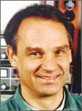
Gerd Binnig, an IBM Fellow and Nobel Laureate, gave the plenary lecture on Monday morning, entitled: “Nanotechnology: The Path to Handling Complexity?” He began his talk by introducing the Millipede project at IBM and mentioned that the project was divided into two groups: signal processing/coding and micro/nanomechanics. Binnig first made a comparison between the stylus record player (turntable) and the atomic force microscope (AFM). Subsequent developments by Don Eigler’s group at IBM on the use of a scanning tunneling microscope (STM) for moving atoms around were then highlighted. These points set the stage for a discussion of nanotechnology as the theme of this lecture.
Dr. Binnig underlined the advantages of the next-generation nanoprocessor chip in terms of being smaller, faster, denser, and potentially cheaper. He used a particularly vivid visual model by zooming in at various magnifications on a pattern. While at very high magnifications, the relationship of each element (pixel) to its immediate neighbors and to the overall picture remained obtuse, at lower magnifications, the objects began to assume a collective significance. Dr. Binnig used this visual aid to underline the fact that thinking is a complex procedure, which is needed to tackle a complex world. Machines that are able to handle this level of complexity can be regard as “intelligent” and they can support our thinking capabilities. The need for such (artificial) intelligent tools will grow as new forms of complexity evolve in terms of a network of highly specialized parallel processing units.
For machines to think intelligently, new paradigms for software and hardware architectures are required. One such approach is the Millipede, which uses thousands of nano-sharp tips to punch indentations (representing individual bits) in a thin plastic film. These indentations can be annealed so that the storage technology is rewritable and can be operated at low power. A 32 x 32 array chip with a density of 100-200 Gbits/in2 was demonstrated. Because a nanometer scale tip can address individual atoms (i.e., has atomic resolution), Dr. Binnig claimed that even further improvements into the Tbit/in2 domain (40 nm bit size) were possible. He ended his lecture with a video clip of the Millipede technology.
This was a fascinating talk by an immensely gifted scientist; those present at this lecture were truly fortunate to have heard him speak. Indeed, this talk kicked off the meeting in fine style.
