Deadline for Submitting Abstracts
March 16, 2018
Submit today!
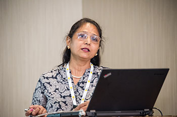 Topic Close-up #7
Symposium H07: Electronic, Thermal, and Electrochemical Properties of Metal Organic Frameworks (MOFs): Technology, Applications, and Emerging Devices
Symposium Focus: The 1st International Symposium sponsored by the Electronics and Photonics Division of the Electrochemical Society brings together researchers in chemistry, materials science, physics, devices and process engineers and related interdisciplinary areas, to seek and capture the state-of-the art in MOF based fundamental aspects and latest technological applications. This symposium offers a new interdisciplinary and international platform, and aims to contribute towards advancing the fundamental understanding of the layered MOF thin films and aiming to improve technological applications thereof. Original contributions are solicited that cover all fundamental and applied aspects including electronic, thermal and electrochemical transport properties and phenomena, device/ system fabrication and integration of MOF thin films into emerging technological device applications. All oral presentations will be grouped into topical sessions. Invited Keynote speakers will present critical reviews covering recent advances and future directions in the diverse field of fundamental and applied MOF properties.
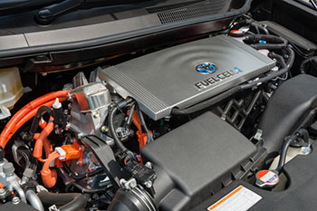 Using advanced computational methods, University of Wisconsin–Madison materials scientists have discovered new materials that could bring widespread commercial use of solid oxide fuel cells closer to reality.
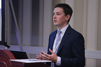 Topic Close-up #6
 A collaborative team of researchers from Shinshu University in Japan have found a new way to curb some of the potential dangers posed by lithium ion batteries.
 Topic Close-up #5
 Topic Close-up #4
 Deadline Extended: March 19, 2018
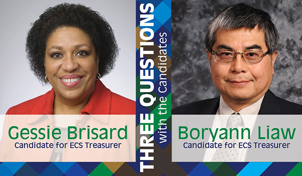 The 2018 Society elections are upon us and ECS wants you to learn more about the candidates, from the candidates. All voting members are eligible to participate via electronic proxy. You would have received an email with voting instructions January 15, 2018.