Shortcut to Solar Cells

black-silicon

The newly developed black silicon has the potential to simplify the manufacturing of solar cells due to the ability of the material to more efficiently collect light.
Image: Barron Group

One of the roadblocks in developing a new, clean energy infrastructure lies in our ability to manufacture solar cells with ease and efficiency. Now, researchers from Rice University may have developed a way to simplify this process.

In Andrew Barron’s Rice University lab, he and postdoctoral student Yen-Tien Lu are developing black silicon by employing electrodes as catalysts.

The typical solar cell is made from silicon. By swapping that regular silicon for black silicon, solar cells gain a highly textured surface of nanoscale spikes that allows for a more efficient collection of light.

This from Rice University:

Barron said the metal layer used as a top electrode is usually applied last in solar cell manufacturing. The new method known as contact-assisted chemical etching applies the set of thin gold lines that serve as the electrode earlier in the process, which also eliminates the need to remove used catalyst particles.

(more…)

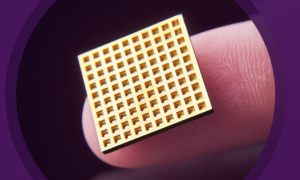
The high-performance 3D microbattery is suitable for large-scale on-chip integration.Image: Engineering at Illinois

The high-performance 3D microbattery is suitable for large-scale on-chip integration.
Image: Engineering at Illinois

Engineers from the University of Illinois at Urbana-Champaign’s College of Engineering have developed a high-performance 3D microbattery applicable for large-scale on-chip integration with microelectronic devices.

“This 3D microbattery has exceptional performance and scalability, and we think it will be of importance for many applications,” said Paul Braun, professor of materials science and engineering at Illinois.

“Micro-scale devices typically utilize power supplied off-chip because of difficulties in miniaturizing energy storage technologies. A miniaturized high-energy and high-power on-chip battery would be highly desirable for applications including autonomous microscale actuators, distributed wireless sensors and transmitters, monitors, and portable and implantable medical devices.”

(more…)

One Step Closer to Bionic Brain

New research shows that we’re one step closer to being able to replicate the human brain outside of the body, which could lead to life-altering research into common conditions such as Alzheimer’s and Parkinson’s disease.

Project leader and ECS published author Sharath Sriram and his group have successfully engineered an electronic long-term memory cell, which mimics the way the human brain processes information.

“This is the closest we have come to creating a brain-like system with memory that learns and stores analog information and is quick at retrieving this stored information,” Sharath said.

(more…)

Top 10 Scientists to Follow on Twitter

Here at ECS, we strive to encourage research, discussion, critical assessment, and dissemination of scientific knowledge. What better way to do that in the digital age than with social networks?

Twitter has been one channel that scientists have adopted in the pursuit of disseminating information and advancing the science though education. Accordingly, we’ve compiled a short list of some of the best scientists to follow on Twitter.

Donald Sadoway, @dsadoway
Professor of Material Chemistry at MIT
ECS member Donald Sadoway is a battery expert and renewable energy guru. Check him out on Twitter to learn about the latest developments in battery technology and current issues in energy and climate.

(more…)

We recently sat down with the University of Iowa’s Johna Leddy, an established researcher in electrochemical power sources and a highly respected mentor to the students of the Leddy Lab. Listen as we talk about the energy infrastructure, Dr. Leddy’s career in academia, how to make the world a better place, and more!

Listen below and download this episode and others for free through the iTunes Store, SoundCloud, or our RSS Feed.

(more…)

Nanoporous gold features high effective surface area, tunable pore size, and high electrical conductivity and compatibility with traditional fabrication techniques.Image: Ryan Chen/LLNL

Nanoporous gold features high effective surface area, tunable pore size, and high electrical conductivity and compatibility with traditional fabrication techniques.
Image: Ryan Chen/LLNL

Researchers from Lawrence Livermore National Laboratory and the University of California, Davis have recently published a paper showing that covering an implantable neural electrode with nanoporus gold could potentially eliminate the risk of scar tissue forming over the electrode’s surface.

Two former ECS member, Erkin Seker and Juergen Biener, were among the researchers involved with this development.

This from Lawrence Livermore National Laboratory:

The team demonstrated that the nanostructure of nanoporous gold achieves close physical coupling of neurons by maintaining a high neuron-to-astrocyte surface coverage ratio. Close physical coupling between neurons and the electrode plays a crucial role in recording fidelity of neural electrical activity.

(more…)

riceuniversity

Researchers were able to deform the molybdenum disulfide without breaking it.
Image: Nano Letters

Many labs have had their eye on molybdenum disulfide recently due to its promising semiconducting properties. Rice University has also turned its attention toward this 2D material and its interesting sandwich structure. During their studies, the researchers have concluded that under certain conditions, molybdenum disulfide can transform from the consistency of peanut brittle to that of taffy.

According to their research, the scientists state that when exposed to sulfur-infused gas at the right temperature and pressure, molybdenum disulfide takes on the qualities of plastic. This development has the potential to have a high impact in the world of materials science.

The structure of the molybdenum disulfide is similar to a sandwich, with layers of sulfur above and below the molybdenum atoms. When the two sheets join at different angles “defective” arrangements—or dislocations—are formed.

(more…)

Each doll housed a phonograph that was activated by a crank on the doll's back.Image: John Reed/National Park Service

Each doll housed a phonograph that was activated by a crank on the doll’s back.
Image: John Reed/National Park Service

Beth Schademann, ECS Publications Specialist, recently came across an NPR article regarding one of ECS’s most famous members and his slightly terrifying, obscure invention.

We talk quite a bit about Thomas Edison here at ECS. Edison happens to be one of our earliest and most recognizable members, not to mention a prolific inventor and entrepreneur.

While Edison is most known for his inventions related to the light bulb and phonograph, he also created the world’s first talking doll back in 1890.

The dolls still exist, but it wasn’t possible to hear the recordings on their tiny phonographs until now. Although, we may have been better off if we never heard these creepy renditions of classic children’s songs.

Edison wasn’t trying to take over the doll market with these toys, he was instead attempting to market his new wax cylinder phonograph for people to use in their homes.


If you also find these recording a bit unsettling, you’re not alone—Edison himself even found them unpleasant. After the dolls flopped in the market due to their high price ($200 in today’s currency) and creepy nature, Edison stopped manufacturing them after only two months.

A curator from the Thomas Edison National Historical Park states that after the dolls went under, Edison refereed to them as his “little monsters.”

(more…)

One of the world’s strongest natural materials has met one of the strongest artificial materials.

Researchers from the University of Trento, Italy conduced an experiment where they sprayed spiders—producers of naturally strong silk—with carbon-based graphene. Why? Curiosity, of course—the backbone of much great science.

From the experiment, the researchers found that some spiders produced silk that was 3.5 times tougher and stronger than the best naturally produced silk.

(more…)

While CNT alignment is still not perfect, it will now be able to be scaled up for large-scale production.Source: North Carolina State University

While CNT alignment is still not perfect, it will now be able to be scaled up for large-scale production.
Source: North Carolina State University

A new process called “microcombing” has been developed to created ultra-strong and highly conductive carbon nanotubes (CNTs).

The films produced from the microcombing technique could have practical applications in improving electronics and aerospace technology.

“It’s a simple process and can create a lightweight CNT film, or ‘bucky paper,’ that is a meter wide and twice as strong as previous such films—it’s even stronger than CNT fibers,” said Yuntian Zhu, Distinguished Professor of Material Science and Engineering at NC State.

(more…)