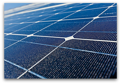
 Researchers have created a concentrating photovoltaic (CPV) system with embedded microtracking that is capable of producing 50 percent more energy per day than the standard silicon solar cells.
“Solar cells used to be expensive, but now they’re getting really cheap,” says Chris Giebink, an assistant professor of electrical engineering at Penn State.
“As a result, the solar cell is no longer the dominant cost of the energy it produces. The majority of the cost increasingly lies in everything else—the inverter, installation labor, permitting fees, etc.—all the stuff we used to neglect,” he says.
This changing economic landscape has put a premium on high efficiency. In contrast to silicon solar panels, which currently dominate the market at 15 to 20 percent efficiency, concentrating photovoltaics focus sunlight onto smaller, but much more efficient solar cells like those used on satellites, to enable overall efficiencies of 35 to 40 percent.


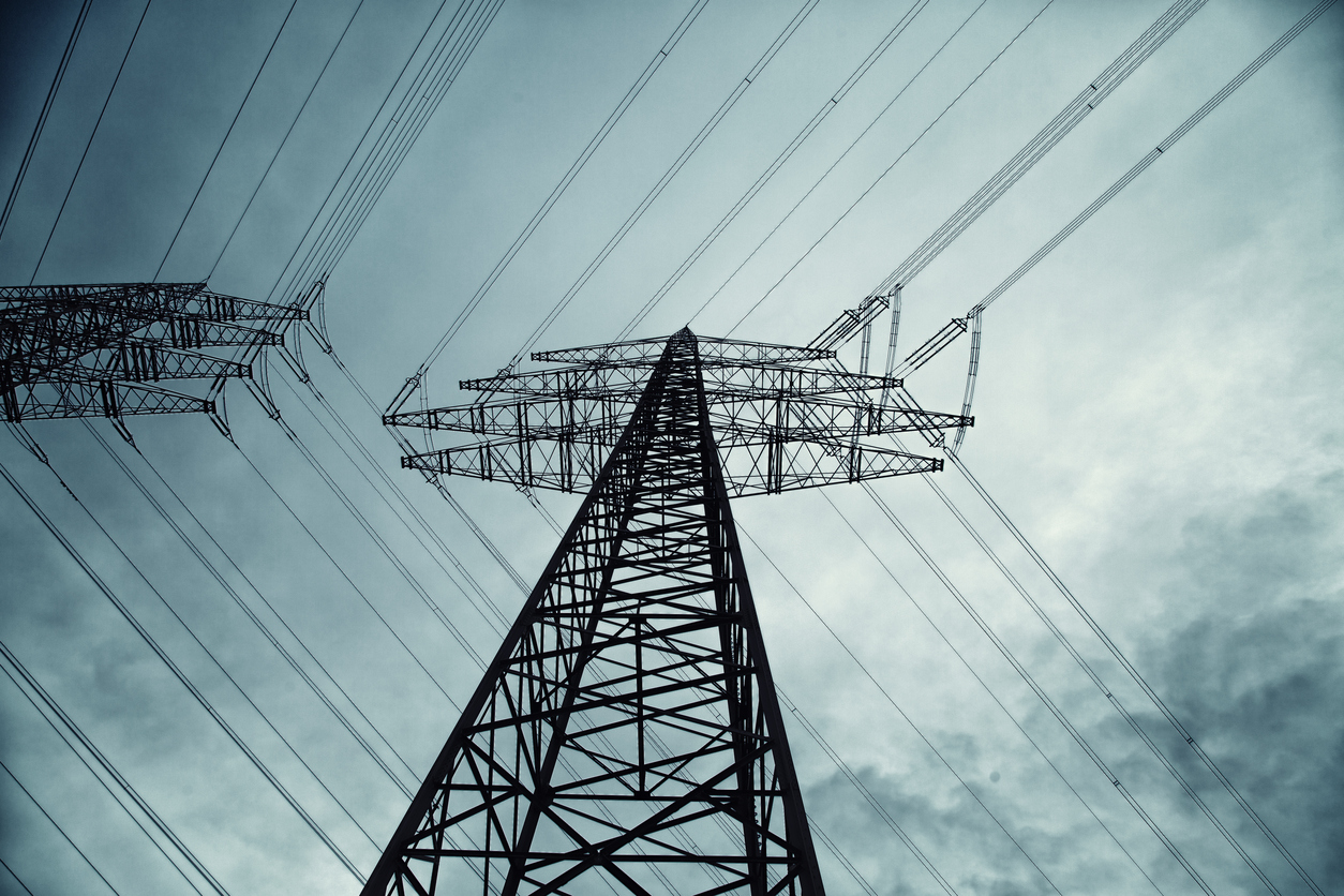 In an effort to expand South Australia’s renewable energy supply, the state has looked to business magnate Elon Musk to build the
  Researchers have developed a new kind of semiconductor alloy capable of capturing the near-infrared light located on the edge of the visible light spectrum.
 In its first “
 The U.S. Department of Energy spends
  The
The  When a battery is used, electrically charged ions travel between electrodes, causing those electrodes to shrink and swell. For some time, researchers have wondered why the electrode materials – which are fairly brittle – don’t crack in the expansion and contraction styles.