Wrinkles and crumples, introduced by placing graphene on shrinky polymers, can enhance graphene's properties.Image: Brown University

Wrinkles and crumples, introduced by placing graphene on shrinky polymers, can enhance graphene’s properties.
Image: Brown University

By now we’ve heard about the seemingly endless possibilities for the wonder material graphene. The engineers at Brown University are looking to make those possibilities even more appealing through a process that could make the nanomaterial both water repellant and enhance its electrochemical properties.

The research team is looking to improve upon the already impressive graphene by wrinkling and crumpling sheets of the material by placing it on shrink polymers to enhance its properties, potentially leading to new breakthroughs in batteries and fuel cells.

This from Brown University:

This new research builds on previous work done by Robert Hurt and Ian Wong, from Brown’s School of Engineering. The team had previously showed that by introducing wrinkles into graphene, they could make substrates for culturing cells that were more similar to the complex environments in which cells grow in the body. For this latest work, the researchers led by Po-Yen Chen, a Hibbit postdoctoral fellow, wanted to build more complex architectures incorporating both wrinkles and crumples.

Read the full article.

Crumpling the graphene makes it superhydrophobic, a property that could be used to develop self-cleaning surfaces. Additionally, the enhanced electrochemical properties could be used in next-generation energy storage and production.

“You don’t need a new material to do it,” said Po-Yen Chen, co-author of the study. “You just need to crumple the graphene.”

Call for Papers: 2D Materials

Focus IssuesJSS Technical Editors: Fan Ren and Stefan De Gendt
and
Guest Editors: Lain-Jong (Lance) Li and Daniel S. P. Lau

invite you to submit to the:
JSS Focus Issue:
Properties, Devices, and Applications Based on 2D Layered Materials

Submission Deadline | May 18, 2016

This special issue of the ECS Journal of Solid State Science and Technology focuses on properties, devices, and applications of two-dimensional (2D) based materials including boron nitrides, black phosphorous, transition metal dichalcogenides/oxides, and other layered materials beyond graphene.

Review and contributed papers are welcome in the following domains:

  • Materials preparation
  • Novel growth technology
  • Growth chemistry
  • Metal contacts
  • Surface cleaning and passivation
  • Wet and dry etching
  • Device design and processing integration
  • Device Physics
  • Device and growth simulation
  • Applications of 2D material based devices and systems
  • Heterostructures based on 2D materials

Submission Deadline | May 18, 2016

Please submit manuscripts at http://ecsjournals.msubmit.net

(Be sure to specify your submission is for the JSS Focus Issue on Properties, Devices, and Applications Based on 2D Layered Materials.)

Papers accepted into this focus issue are published online within 10 days of acceptance. The issue is created online an article at a time with the final article published in October 2016.

New Semiconductor Material for Faster Electronics

The newly developed semiconductor material could eventually lead to electronic devices that are 100 percent faster.
Image: Dan Hixson/University of Utah College of Engineering

Thanks to a new development in semiconducting materials, our electronics may soon be faster all while consuming a lot less power.

The semiconductor is comprised of tin and oxygen and is only one atom thick, which allows electrical charges to move very quickly – much faster than comparable materials, such as silicon. This material also differs from conventional 3D materials, as it is 2D. The benefit of this material being 2D lies in the reduction of layers and thickness, thus allowing electronics to move faster.

This material has the ability to be applied to transistors, which are central to the majority of electronic devices.

This from the University of Utah:

While researchers in this field have recently discovered new types of 2D material such as graphene, molybdenun disulfide and borophene, they have been materials that only allow the movement of N-type, or negative, electrons. In order to create an electronic device, however, you need semiconductor material that allows the movement of both negative electrons and positive charges known as “holes.” The tin monoxide material discovered by Tiwari and his team is the first stable P-type 2D semiconductor material ever in existence.

(more…)

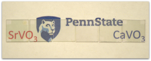
penn-state-materialA new material developed at Penn State could mean big things for everything from smartphones to solar cells.

For over 60 years, the main material used in transparent conductor display has been indium tin oxide. With over 90 percent of the display market utilizing this material, it has left very little room for competitor materials.

While indium tin oxide has provided solid efficiency levels at a decent price point for the past half decades, expenses have recently skyrocketed on this material.

Current electronic devices, such as smart phones and tables, are primarily priced according to display material costs. Displays and touch screen modules make up 40 percent of the cost to produce a device, greatly outpacing other essential pieces such as chips and processors. It hasn’t been until now that researchers have found a material that could potential replace indium tin oxide and potentially reduce device costs.

(more…)

World’s Most Expensive Material

The world’s most expensive material is being created in a lab and it’s going for $33,000 per 200 micrograms. To put that in perspective, that’s an astonishing $4.2 billion an ounce.

The novel material consists of molecular units called endohedral fullerenes, which are essentially a cage of carbon atoms containing nitrogen atoms.

Developers and scientists behind the material are focused on implementing the endohedral fullerenes into the development of a small, portable atomic clock. The atomic clock is the most accurate time-keeping system in the world and could assist in the accuracy of everything from a GPS to an automatic car.

“Imagine a minaturised atomic clock that you could carry around in your smartphone,” says Kriakos Porfyrakis, scientist working on the development of the material. “This is the next revolution for mobile.”

Aside from impacting cellphone technology, Porfyrakis expects the material to change transportation in a big way.

ICYMI: Learn about the early history of the Buckyball.

“There will be lots of applications for this technology,” says Lucius Cary, director of Oxford Technology SEIS fund. “The most obvious is in controlling autonomous vehicles. If two cars are coming towards each other on a country lane, knowing where they are to within 2m is not enough but to 1mm it is enough.”

New Phase of Carbon Shows Unique Properties

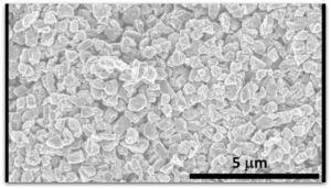
q-carbonA new form of carbon that has unprecedented strength and magnetism properties is making its mark in the world of materials science.

Researchers from North Carolina State University have recently developed a new phase of carbon called Q-carbon—an extraordinarily strong material that differs from carbon’s other two solid forms.

The first solid phase of carbon is graphite. Graphite is composed by lining up carbon atoms to form thin sheets, which results in a thin and flaky material. The other phase of carbon, diamond, occurs when carbon atoms form a rigid crystal lattice.

Third Phase of Carbon

“We’ve now created a third solid phase of carbon,” says Jay Narayan, lead author of the research. “The only place it may be found in the natural world would be possibly in the core of some planets.”

Q-carbon differs from both existing phases of carbon, with unique characteristics that researchers did not even think were possible prior to its development, such as its magnetic and glowing qualities. To fully understand its novel qualities, it’s essential to understand how Q-carbon was developed.

(more…)

Nanoporous Materials and Global Warming

In a practical effort to address climate change, researchers are looking at the possibility to capture harmful greenhouse gasses and transforming them into something useful for society. Recently, researchers from the University of South Carolina started exploring this topic, opening the door for more research in green fuels produced by carbon. Now, a team from the University of South Australia is taking that concept and applying nanoporous carbon nitride to help solve global warming.

With carbon dioxide levels at their highest in 650,000 years, scientists are developing innovative ways to help contain the greenhouse gas. The team at the University of South Australia, led by Ajayan Vinu, is working to capture and convert carbon dioxide molecules with the help of nanoporous materials.

“Their interesting properties—a semiconducting framework structure and ordered pores—make them exciting candidates for the capture and conversion of [carbon dioxide] molecules into methanol which can then be used as a source of green energy with the help of sunlight and water,” Vinu said.

(more…)

Powering Batteries in Harsh Environments

Researchers across the globe have been investing more and more effort into developing new materials to power the next generation of devices. With the population growing and energy demands rising, the need for smaller, faster, and more efficient batteries is more prevalent than ever.

While some researchers are attempting to develop complex material combinations to tackle this issue, researchers from Rice University are going back to basics by developing a clay-based electrolyte.

Utilizing clay as a primary material in a lithium ion battery could address current issues that the battery has with high temperature performance. With clay, the researchers were able to supply stable electrical power in environments with temperatures up 120°C. The addition of clay to the electrode could allow lithium ion batteries to function in harsh environments including space, defense, and oil and gas applications.

(more…)

New Approach to Materials Design

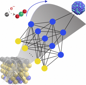
jz-2015-016605_0003A novel development from Virginia Tech aims to “significantly accelerate materials discovery,” all while combating the pressing global warming issue.

The new approach allows for efficient chemical conversions through a model that can predict novel alloy materials in a fast and accurate manner.

“This is the first example of learning from data in catalysis. We anticipate that this new research approach will have a huge impact in the future of materials design,” said Honglian Xin, lead author of the study.

Catalysts are hugely important in industry, with up to 90 percent of industrial chemicals being made from catalysts. These catalysts range from acids to nanoparticles, and even make up some enzymes in the human body.

Scientists have previously worked to improve catalysts through mixing metals with very precise atomic structures. While the results of these studies have led to metals with promising physical and chemical properties, the process has been costly and time consuming.

This from Virginia Tech:

That is why [the researchers] decided to use existing data to train computer algorithms to make predictions of new materials, a field called machine learning. The approach captures complex, nonlinear interactions of molecules on metal surfaces through artificial neural networks, thus allowing, “large scale exploration alloy materials space,” according to their article.

(more…)

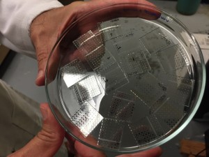
The new hybrid sol-gel material provides an electrical energy storage capacity rivaling some batteries.Image: John Toon/Georgia Tech

The new hybrid sol-gel material provides an electrical energy storage capacity rivaling some batteries.
Image: John Toon/Georgia Tech

The future of electric vehicle and defibrillator technologies depend largely on new, innovative energy storage research and improving device power densities. With the high demand for more powerful, efficient energy devices, the researchers from Georgia Tech believe they may have developed what could be the answer to powering large-scale devices.

The team has developed a new capacitor dielectric material. This capacitor—developed from a hybrid silica sol-gel material and self-assembled monolayers of common fatty acid—has the potential to surpass some of today’s conventional batteries in the field of energy and power density.

If the researchers can scale up their current laboratory sample, the new capacitors will be able to provide large amounts of current quickly to large-scale applications.

This from Georgia Tech:

The new material is composed of a silica sol-gel thin film containing polar groups linked to the silicon atoms and a nanoscale self-assembled monolayer of an octylphosphonic acid, which provides insulating properties. The bilayer structure blocks the injection of electrons into the sol-gel material, providing low leakage current, high breakdown strength and high energy extraction efficiency.

(more…)

  • Page 5 of 8