The new polymer is able to store energy at higher temperatures.Image: Qi Li/Nature

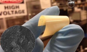
The new polymer is able to store energy at higher temperatures.
Image: Qi Li/Nature

Polymer dielectric materials have many beneficial properties when it comes to energy storage for advanced electronics and power systems. While the materials are highly flexible and have good chemical stability, their main drawback is their limitation of functionality in primarily low working temperatures. In turn, this limits the wider use of polymer dielectric materials for applications such as electric vehicles and underground oil exploration.

However, researchers from Pennsylvania State University have developed a flexible, high-temperature dielectric material from polymer nanocomposites that looks promising for the application of high-temperature electronics.

The researchers, including current ECS member Lei Chen, were able to stabilize dielectric properties by crosslinking polymer nanocomposites that contain boron nitride nanosheets. In testing, the energy density was increased by 400 percent while remaining stable at temperatures as high as 300° C.

With the nanocomposites having huge energy storage capabilities at high temperatures, a much broader application of organic materials in high temperatures electronics and energy storage can be explored.

PS: Interested in polymer research? Make sure to attend the 228th ECS Meeting and get the latest polymer science at our polymers symposia.

96416_web

Mario Hofmann of National Cheng Kung University shows the example set up of electrochemical synthesis.
Image: Mario Hofmann/IOP Publishing

Graphene has been affectionately coined the “wonder material” due to its strength, flexibility, and conductive properties. The theoretical applications for graphene have included the five-second phone charge, chemical sensors, a way to soak up environmentally harmful radioactive waste, and even the potential to improve your tennis game. While everyone has big expectations for the wonder material, it’s still struggling to find its place in the world of materials science.

However, a team of researchers may have found a way to expand graphene’s potential and make it more applicable to tangible devices and applications. Through a simple electrochemical approach, researchers have been able to alter graphene’s electrical and mechanical properties.

Technically, the researchers have created a defect in graphene that can make the material more useful in a variety of applications. Through electrochemical synthesis, the team was able to break graphite flakes into graphene layers of various size depending on the level of voltage used.

The different levels of voltage not only changed the material’s thickness, it also altered the flake area and number of defects. With the alternation of these three properties, the researchers were able to change how the material acts in different functions.

“Whilst electrochemistry has been around for a long time it is a powerful tool for nanotechnology because it’s so finely tuneable.” said Mario Hofmann, a researcher at National Cheng Kung University in Taiwan, in a press release. “In graphene production we can really take advantage of this control to produce defects.”

The defected graphene shows promising potential for polymer fillers and battery electrodes. Researchers also believe that by revealing and utilizing the natural defects in graphene, strides could be made in biomedical technology such as drug delivery systems.

Using this National Geographic image, Dr. Chanda is able to demonstrate the color-changing abilities of the nanostructured reflective display.Image: University of Central Florida

Using this National Geographic image, Dr. Chanda is able to demonstrate the color-changing abilities of the nanostructured reflective display.
Image: University of Central Florida

The development to the first colorful, flexible, skin-like display is taking wearable electronics to a whole new level.

Researchers from the University of Central Florida’s NanoScience Technology Centre have created a digital “skin” that can cloak wearers in realistic images. This new technology could be applied to concepts as simple as outfit changes, or more serious matters like replacing camouflage for members of the military.

The research was led by Professor Debashis Chanda, who took inspiration for this development from nature.

“All manmade displays – LCD, LED, CRT – are rigid, brittle and bulky. But you look at an octopus, they can create color on the skin itself covering a complex body contour, and it’s stretchable and flexible,” Chanda said. “That was the motivation: Can we take some inspiration from biology and create a skin-like display?”

This from Wired:

The result is described as an ultra-thin nanostructure, which can change color when different voltage is applied. The method uses ambient light rather than its own light source, meaning no bulky backlighting is needed, and the structure is relatively simple; a thin liquid crystal layer above and metallic “egg carton” like nanomaterial that reflects wavelengths selectively.

Read the full article here.

In the end, the researchers developed something that is 25 times thinner than human hair for easy application to fabrics and plastics.

Head over to the Digital Library to read about some of the latest research and innovations in nanomaterials.

Analyzing Thin Film Break-Up

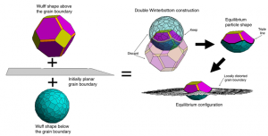
The open-source code, WulffMaker, is available as a Wolfram computable document format file or a Mathematica notebook.Image: MIT/Rachel Zucker

The open-source code, WulffMaker, is available as a Wolfram computable document format file or a Mathematica notebook.
Image: MIT/Rachel Zucker

Recent PhD recipient and past ECS student member, Rachel Zucker, examined one of the most complex issues in materials science and has developed a range of mathematical solutions to explain the phenomena known as “dewetting” in solid films. In defense of her thesis, Zucker modeled dewetting in microscale and nanoscale thin films.

Dewetting can be boiled down to the general break-up of material due to excess surface energy. Zucker’s development provides us with not only a new understanding of this phenomenon, but also a way to simulate it. When analyzing solid state dewetting, issues becomes very prominent as engineers attempt to make products with smaller and smaller features.

“The big takeaway is: One, we can write down formulation of this problem; two, we can implement a numerical method to construct the solutions; three, we can make a direct comparison to experiments; and that strikes me as what a thesis should be — the complete thing — formulation, solution, comparison, conclusion,” said W. Craig Carter, MIT professor and Zucker’s co-adviser.

(more…)

Join the ECS Montreal Student Chapter for the 5th ECS Montreal Student Symposium.

Montreal Student Chapter Symposium 2015

This is an annual meeting for electrochemistry and materials science students in Montreal, Canada.

Abstract submission is now open until May 27, 2015. Submissions may be emailed here.

(more…)

Shortcut to Solar Cells

black-silicon

The newly developed black silicon has the potential to simplify the manufacturing of solar cells due to the ability of the material to more efficiently collect light.
Image: Barron Group

One of the roadblocks in developing a new, clean energy infrastructure lies in our ability to manufacture solar cells with ease and efficiency. Now, researchers from Rice University may have developed a way to simplify this process.

In Andrew Barron’s Rice University lab, he and postdoctoral student Yen-Tien Lu are developing black silicon by employing electrodes as catalysts.

The typical solar cell is made from silicon. By swapping that regular silicon for black silicon, solar cells gain a highly textured surface of nanoscale spikes that allows for a more efficient collection of light.

This from Rice University:

Barron said the metal layer used as a top electrode is usually applied last in solar cell manufacturing. The new method known as contact-assisted chemical etching applies the set of thin gold lines that serve as the electrode earlier in the process, which also eliminates the need to remove used catalyst particles.

(more…)

riceuniversity

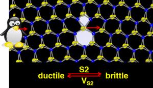
Researchers were able to deform the molybdenum disulfide without breaking it.
Image: Nano Letters

Many labs have had their eye on molybdenum disulfide recently due to its promising semiconducting properties. Rice University has also turned its attention toward this 2D material and its interesting sandwich structure. During their studies, the researchers have concluded that under certain conditions, molybdenum disulfide can transform from the consistency of peanut brittle to that of taffy.

According to their research, the scientists state that when exposed to sulfur-infused gas at the right temperature and pressure, molybdenum disulfide takes on the qualities of plastic. This development has the potential to have a high impact in the world of materials science.

The structure of the molybdenum disulfide is similar to a sandwich, with layers of sulfur above and below the molybdenum atoms. When the two sheets join at different angles “defective” arrangements—or dislocations—are formed.

(more…)

One of the world’s strongest natural materials has met one of the strongest artificial materials.

Researchers from the University of Trento, Italy conduced an experiment where they sprayed spiders—producers of naturally strong silk—with carbon-based graphene. Why? Curiosity, of course—the backbone of much great science.

From the experiment, the researchers found that some spiders produced silk that was 3.5 times tougher and stronger than the best naturally produced silk.

(more…)

Mimicking Nature’s Camouflage

In the world of ocean life, the cuttlefish is the king of camouflage. The cuttlefish’s ability to disguise itself, becoming virtually invisible to the naked eye, is an amazing quality that is very difficult to engineer. But with a little inspiration from marine animal, engineers from the University of Nebraska-Lincoln (UNL) have developed a design that mimics patters and textures in a flash.

Within seconds of light exposure, the new structure begins to replicate color and texture of the surrounding environment. While engineers have developed camouflaging materials before, this new design responds to much lower-intensity light and at faster rates than the few predecessors that exist.

“This is a relatively new community of research,” said Li Tan, associate professor of mechanical and materials engineering. “Most of the people (in it) are inspired by the cuttlefish, whose skin changes color and texture, as well.”

(more…)

Ushering in Next-Gen Batteries, Fuel Cells

ECS member

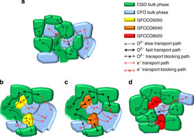
ECS member Shumin Fang was a contributor in a development that could dramatically improve the efficiency of batteries and fuel cells.
Image: Nature Communications

Sometimes the tiniest things could have the biggest impact—especially when it comes to battery technology.

New research from a collaborative team of engineers from Clemson University and the University of South Carolina developed a new material that could boost batteries’ power and help power plants.

ECS student member Shumin Fang of the University of South Carolina was a collaborator on the study. (Take a look at his paper on solid oxide fuel cells.)

The new material acts as a superhighway for ions, allowing for more powerful batteries and boosting the general efficiency of energy conversion.

Because batteries and fuel cells are limited by how fast ions can pass through the electrolyte, engineers must find a mix of electrolyte ingredients that allows for fast movement. This study proposes the answer to this in gadolinium doped ceria.

(more…)

  • Page 6 of 8