
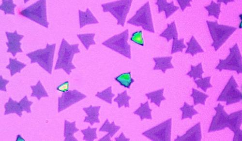
The researchers discovered that two flat semiconductor materials can be connected edge-to-edge with crystalline perfection.
Credit: University of Washington
Current member of ECS, Xiaodong Xu, has made a huge contribution to the field of electrochemical science with the creation of atomically seamless, thinnest-possible semiconductor junctions.
Xu, along with the scientists at the University of Washington, believe their semiconductor – coming in at only three atoms thick – is the most slender possible, a new class of nanoscale materials.
This from the University of Washington:
The University of Washington researchers have demonstrated that two of these single-layer semiconductor materials can be connected in an atomically seamless fashion known as a heterojunction. This result could be the basis for next-generation flexible and transparent computing, better light-emitting diodes, or LEDs, and solar technologies.
“Our experimental demonstration of such junctions between two-dimensional materials should enable new kinds of transistors, LEDs, nanolasers, and solar cells to be developed for highly integrated electronic and optical circuits within a single atomic plane,” Xu said.
The research was published online this week in Nature Materials.
Find more research from Xu published in our Digital Library.