Andy GroveBusinessman, author, and one of the foremost minds behind the development of the semiconductor, Andy Grove, passed away on Monday at the age of 79.

Technological giant

During his three decades with Intel, Grove helped transform the chip-making colossus into the world’s largest manufacturer of semiconductors. He grew with the company as it obtained more and more success, acting as Intel’s president in 1979 and becoming CEO in 1987.

“We are deeply saddened by the passing of former Intel Chairman and CEO Andy Grove,” said current Intel CEO Brian Krzanich in a news release. “Andy made the impossible happen, time and again, and inspired generations of technologists, entrepreneurs, and business leaders.”

Many considered Grove as one of the giants in the world of technology, leaving his mark on everything from memory chips to the digital revolution at large. Without Grove’s contributions to the development of the semiconductor, much of modern life would be very different. Items such as handheld electronics, LED displays, and even solar cells would not exist if not for the semiconductor.

(MORE: Learn about how semiconductors shape society.)

Grove’s influence on ECS

Here at ECS, Grove’s contributions to technology have helped shape some of our divisions and topical interest areas. In 2013, the Society established the Bruce Deal & Andy Grove Young Author Award to recognize the best paper published in the ECS Journal of Solid State Science and Technology (JSS) by a young author. The award was named in Deal, another Fairchild employee, and Grove’s honor for a seminal paper that was published in the Journal of The Electrochemical Society (JES) describing the Deal-Grove model, which is used to analyze thermal oxidation of silicon in semiconductor device fabrication and has had a lasting influence on the semiconductor technology industry.

(more…)

New Semiconductor Material for Faster Electronics

The newly developed semiconductor material could eventually lead to electronic devices that are 100 percent faster.
Image: Dan Hixson/University of Utah College of Engineering

Thanks to a new development in semiconducting materials, our electronics may soon be faster all while consuming a lot less power.

The semiconductor is comprised of tin and oxygen and is only one atom thick, which allows electrical charges to move very quickly – much faster than comparable materials, such as silicon. This material also differs from conventional 3D materials, as it is 2D. The benefit of this material being 2D lies in the reduction of layers and thickness, thus allowing electronics to move faster.

This material has the ability to be applied to transistors, which are central to the majority of electronic devices.

This from the University of Utah:

While researchers in this field have recently discovered new types of 2D material such as graphene, molybdenun disulfide and borophene, they have been materials that only allow the movement of N-type, or negative, electrons. In order to create an electronic device, however, you need semiconductor material that allows the movement of both negative electrons and positive charges known as “holes.” The tin monoxide material discovered by Tiwari and his team is the first stable P-type 2D semiconductor material ever in existence.

(more…)

Building Better Electronic Devices

The development of the silicon chip forever changed the field of electronics and the world at large. From computers to cellphones to digital home appliances, the silicon chip has become an inextricable part of the structure of our society. However, as silicon begins to reach its limits many researchers are looking for new materials to continue the electronics revolution.

Fan Ren, Distinguished Professor at the University of Florida and Technical Editor of the ECS Journal of Solid State Science and Technology, has based his career in the field of electronics and semiconductor devices. From his time at Bell Labs through today, Ren has witnessed much change in the field.

Future of Electronics

Upon coming to the United States from Taiwan, Ren was hired by Bell Labs. This hub of innovation had a major impact on Ren and his work, and is where he first got his hands-on semiconductor research. During this time, silicon was the major player as far as electronic materials went. While electronics have transformed since that time, the materials used to create integrated circuits have essentially stayed the same.

People keep saying of other semiconductors, “This will be the material for the next generation of devices,” says Ren. “However, it hasn’t really changed. Silicon is still dominating.”

(more…)

Call for Papers: JSS Focus Issue

JSS CoverThis special issue of the ECS Journal of Solid State Science and Technology focuses on defect characterization in semiconductor materials and devices. We especially welcome papers in the following domains:

  • Structural, chemical, electrical and optical characterization of extended defects in semiconductor nano-structures and materials
  • Electrical and optical characterization of point defects in semiconductor nano-structures
  • Semiconductor-device-based defect analysis
  • Impact of (extended) defects on device and circuit operation and yield
  • Defect characterization and control in hetero-epitaxial layers and nano-structures grown on Si, comprising Ge, SiGe, GeSn, III-V and III-nitrides
  • Ab initio calculations and TCAD of the electrical activity of (extended) defects in semiconductor materials and devices
  • Defect control and mitigation strategies during hetero-epitaxial deposition

Find out more!

Submission Deadline | Oct. 21, 2015
Papers accepted into this focus issue are published online within 10 days of acceptance.
The issue is created online an article at a time with the final article published in March 2016.

Member Spotlight – Chennupati Jagadish

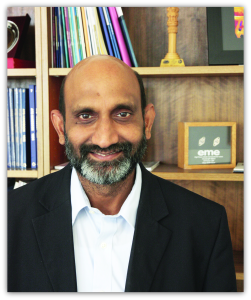
jagadishECS Fellow Chennupati Jagadish has been awarded the IEEE Nanotechnology Pioneer Award for his outstanding contributions to compound semiconductor nanowire and quantum dot optoelectronics.

Dr. Jagadish is a Laureate Fellow and Distinguished Professor at the Australian National University, where he has made major advances in compound semiconductor quantum dot and nanowire growth techniques and optoelectronic devices.

Previously, Dr. Jagadish was awarded the ECS Electronics and Photonics Division Award for his excellence in electronics research outstanding technical contribution to the field of electronics science.

Throughout his scientific career, Dr. Jagadish has published more than 620 research papers—some of which can be found in the Digital Library—and has 5 U.S. patents.

Some of Dr. Jagadish’s current research focuses on nanostructured photovoltaics, which provides novel concepts to produce a more efficient solar cell.

riceuniversity

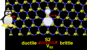
Researchers were able to deform the molybdenum disulfide without breaking it.
Image: Nano Letters

Many labs have had their eye on molybdenum disulfide recently due to its promising semiconducting properties. Rice University has also turned its attention toward this 2D material and its interesting sandwich structure. During their studies, the researchers have concluded that under certain conditions, molybdenum disulfide can transform from the consistency of peanut brittle to that of taffy.

According to their research, the scientists state that when exposed to sulfur-infused gas at the right temperature and pressure, molybdenum disulfide takes on the qualities of plastic. This development has the potential to have a high impact in the world of materials science.

The structure of the molybdenum disulfide is similar to a sandwich, with layers of sulfur above and below the molybdenum atoms. When the two sheets join at different angles “defective” arrangements—or dislocations—are formed.

(more…)

Three Atom Thick Transistor

A new study by two ECS published authors, David Muller and Jiwoong Park, has led to an electronic piece that is just three atoms thick.

The researchers have unveiled a process to develop ultra-thin transistors made from TMD, otherwise known as transition metal dichalcogenide. This material is novel in the fact that it possesses properties that make it a perfect fit for solar cells, light detectors, or semiconductors.

Researchers have been examining TMDs for some time now, but have been finding it difficult to get them to work consistently. This new study has discovered the best process yet to manufacture the materials, which could lead to a breakthrough in the future of electronics and possibly bring about an end to Moore’s law.

(more…)

Water Helps Form Tiniest Wires Ever

The nanowires were created through a process called meniscus-mask lithography.Image: Tour Group/Rice University

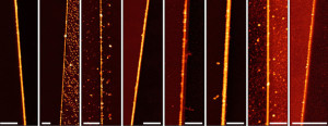
The nanowires were created through a process called meniscus-mask lithography.
Image: Tour Group/Rice University

Scientists and researchers around the world are always looking for ways to improve technology. While we’ve been making smaller circuits to improve semiconductors for some time now, we’ve just about reached the physical limits of shrinking nanowires. However, this newly developed technique allows for the formation of the tiniest wires yet.

A new technique has been developed that uses water to create patterns of wires less than 10 nanometers wide.

“This could have huge ramifications for chip production since the wires are easily made to sub-10-nanometer sizes,” said lead author James M. Tour. “There’s no other way in the world to do this en masse on a surface.”

(more…)

Silicon is the common material used in solar cells and computer chips, but gallium arsenide is an alternative material with many advantages. Image: YouTube/Stanford University

Silicon is the common material used in solar cells and computer chips, but gallium arsenide is an alternative material with many advantages.
Image: YouTube/Stanford University

When we think of chips and solar cells, we think of silicon. However, silicon isn’t the only chip-making material out there.

Researchers from Stanford University are turning their attention away from silicon and are looking toward gallium arsenide to make faster chips and more efficient solar cells.

Gallium arsenide is a semiconductor material with extraordinary properties. Electrons can travel six times faster in gallium arsenide than in silicon, allowing for faster operation of transistors. Unfortunately, cost effectiveness is not one of gallium arsenide’s alluring properties—which has caused researchers to opt for the much cheaper and less effective silicon material.

One single wafer of gallium arsenide could cost up to $5,000, whereas the same size wafer of silicon costs only $5.

(more…)

Member Spotlight – Jim Edgar

Edgar's new patented process will allow for the building of better semiconductors.Source: Kansas State University

Edgar’s new patented process will allow for the building of better semiconductors.
Source: Kansas State University

The Electrochemical Society’s Jim Edgar has developed a new process to build better semiconductors, which will vastly improve the efficiency of electronic devices and help propel the semiconductor industry.

Edgar, a Kansas State university distinguished professor of chemical engineering and an active member of ECS since 1981, has just received a patent for his “Off-axis silicon carbide substrates” process, which is a way to build a better semiconductor. This new process could mean big things for the electronics and semiconductor manufacturing industries.

“It’s like a stacked cake separated by layers of icing,” Edgar said. “When the layers of semiconductors don’t match up very well, it introduces defects. Any time there is a defect, it degrades the efficiency of the device.”

(more…)

  • Page 2 of 3