 A quantum probe based on an atomic-sized “color center” in diamonds has let researchers observe the flow of electric currents in graphene.
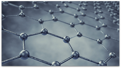
Made up of a lattice of carbon atoms only one atom thick, graphene is a key material for the electronics of the future. The thin carbon material is stronger than steel and due to its flexibility, transparency, and ability to conduct electricity, holds great promise for use in solar cells, touch panels, and flexible electronics.
No one has been able to see what is happening with electronic currents in graphene, says Lloyd Hollenberg, professor at the University of Melbourne and deputy director of the Centre for Quantum Computation and Communication Technology.
According to Hollenberg, this new technique overcomes significant limitations with existing methods for understanding electric currents in devices based on ultra-thin materials.
“The ability to see how electric currents are affected by these imperfections will allow researchers to improve the reliability and performance of existing and emerging technologies,” Hollenberg says. “We are very excited by this result, which brings quantum probe-based imaging to the world of graphene nanoelectronics and quantum computers.”
Quantum computers will harness the power of atoms and molecules to perform memory and processing tasks, and have the potential to perform certain calculations significantly faster than any conventional computer.
But next-generation electronic devices based on ultra-thin materials, including quantum computers, will be especially vulnerable to contain minute cracks and defects that disrupt current flow.
The success of the new sensing technique means researchers now have the potential to observe how electrons move in such tiny structures.
“These observations could aid our future understanding of how quantum computers will operate, as well as contribute to our understanding of electron behavior in new and emerging technologies,” Hollenberg says.
Lead author Jean-Philippe Tetienne of CQC2T explains how the team used diamond to successfully image the current: “Our method is to shine a green laser on the diamond, and see red light arising from the color center’s response to an electron’s magnetic field.”
“By analyzing the intensity of the red light, we determine the magnetic field created by the electric current and are able to image it, and literally see the effect of material imperfections.”
“Our technique is powerful yet relatively simple to implement, which means it could be adopted by researchers and engineers from a wide range of disciplines,” says Tetienne. “Using the magnetic field of moving electrons is an old idea in physics, but this is a novel implementation at the microscale with 21st century applications.”
“Building a device that combined graphene with the extremely sensitive nitrogen vacancy color center in diamond was challenging, but an important advantage of our approach is that it’s non-invasive and robust—we don’t disrupt the current by sensing it in this way,” says Nikolai Dontschuk, a graphene researcher at the University of Melbourne School of Physics.
The current-imaging results appear in Science Advances. Funding comes from the Australian Research Council through the Centre of Excellence and Laureate Fellowship programs.
Source: University of Melbourne
This article was originally published on Futurity.


