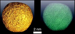
Engineers have developed a way to visualize the optical properties of objects that are thousands of times small than a grain of sand.
Source: YouTube/Stanford University
In order to develop high efficiency solar cells and LEDs, researchers need to see how light interacts with objects on the nanoscale. Unfortunately, light is tricky to visualize in relation to small-scale objects.
Engineers from Stanford University, in collaboration with FOM Institute AMOLF, have developed a next-gen optical method to produce high-resolution, 3D images of nanoscale objects. This allows researchers to visualize the optical properties of objects that are several thousandths the size of a grain of sand.
The teams achieved this by combining two technologies: cathodluminescence and tomography.
This from Stanford University:
By scanning the beam back and forth over the object, the engineers created a 2-D image of these optical properties. Each pixel in this image also contained information about the wavelength of emitted photons across visible and near-infrared wavelengths. This 2-D cathodoluminescence spectral imaging technique, pioneered by the AMOLF team, revealed the characteristic ways in which light interacts with this nanometer-scale object.
The engineers believe that their development could lead to great innovation in the future.
“It has applications for testing various types of engineered and natural materials,” said study lead author Ashwin Atre. “For instance, it could be used in manufacturing LEDs to optimize the way light is emitted, or in solar panels to improve the absorption of light by the active materials.”
The findings are detailed in the journal Nature Nanotechnology.
 If you’re conducting nano research, make sure to submit your abstracts for the 228th ECS Meeting in Phoenix this October! We’ll be hosting symposia on a multitude of topics related to nanotechnology.
Abstracts are due no later than May 1, 2015.

