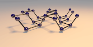
According to new research, black phosphorus may have the potential to outpace silicon.
Image: McGill University
We’re one step closer to atomic layer transistors due to recent research by a team of McGill University and Université de Montréal researchers. The new findings are the result of multidisciplinary work that yielded evidence that the material black phosphorus may make it possible to pack more transistors on a chip.
Researchers from McGill University joined with ECS’s Richard Martel in the Université de Montréal’s Department of Chemistry to examine if black phosphorus could tackle the prominent issue in the electronics field of designing energy-efficient transistors.
Similar to graphite, black phosphorus can be separate easily into single atomic layers to allow for thin transistors. When researchers are able to produce thinner transistors, they are also more efficient.
The process of taking the black phosphorus and forming it into a single-layer material is known in the scientific community as phosphorene. By doing this, it allows the black phosphorus to compete with the wonder material graphene, and even offers solutions to some of the difficulties that graphene cannot overcome when applied to electronics. Black phosphorus is a natural semiconductor so it can be switched on and off, unlike the metal-based behavior of graphene.
“To lower the operating voltage of transistors, and thereby reduce the heat they generate, we have to get closer and closer to designing the transistor at the atomic level,” said Thomas Szkopek, senior author to the study. “The toolbox of the future for transistor designers will require a variety of atomic-layered materials: an ideal semiconductor, an ideal metal, and an ideal dielectric. All three components must be optimized for a well-designed transistor. Black phosphorus fills the semiconducting-material role.”
PS: Richard Martel is a Member-at-Large of ECS’s Nanocarbons Division. Listen to the podcast below and find out more about this historic division and the science associated with it.

