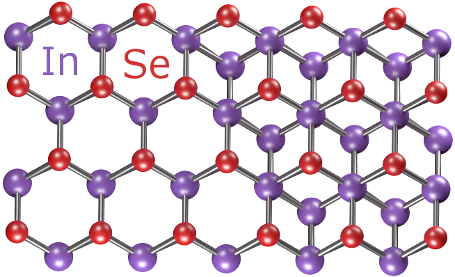
 Newly developed semiconductor materials are showing promising potential for the future of super-fast electronics.
A new study out of the University of Manchester details a new material called Indium Selenide (InSe). Like graphene, InSe if just a few atoms thick, but it differs from the “wonder material” in a few critical ways. While graphene has been hailed for its electronic properties, researchers state that it does not have an energy gap – making graphene behave more like a metal than a semiconductor.
Similarly, InSe can be nearly as thin as graphene while exhibiting electronic properties higher than that of silicon. Most importantly, InSe has a large energy gap, which could open the door to super-fast, next-gen electronic devices.
“Ultra-thin InSe seems to offer the golden middle between silicon and graphene,” says Sir Andre Gemi, co-author of the study and Nobel Prize laurate for his research into graphene. “Similar to graphene, InSe offers a naturally thin body, allowing scaling to the true nanometre dimensions. Similar to silicon, InSe is a very good semiconductor.”
This from Manchester University:
The Manchester researchers had to overcome one major problem to create high-quality InSe devices. Being so thin, InSe is rapidly damaged by oxygen and moisture present in the atmosphere. To avoid such damage, the devices were prepared in an argon atmosphere using new technologies developed at the National Graphene Institute.
This allowed high-quality atomically-thin films of InSe for the first time. The electron mobility at room temperature was measured at 2,000 cm2/Vs, significantly higher than silicon. This value increases several times at lower temperatures.
“The technology that the NGI has developed for separating atomic layers of materials into high-quality two-dimensional crystals offers great opportunities to create new material systems for optoelectronics applications,” says Vladimir Falko, co-author of the study and director of the National Graphene Institute. “We are constantly looking for new layered materials to try.”


