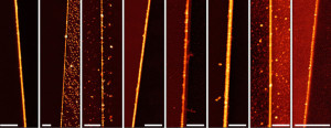
The nanowires were created through a process called meniscus-mask lithography.
Image: Tour Group/Rice University
Scientists and researchers around the world are always looking for ways to improve technology. While we’ve been making smaller circuits to improve semiconductors for some time now, we’ve just about reached the physical limits of shrinking nanowires. However, this newly developed technique allows for the formation of the tiniest wires yet.
A new technique has been developed that uses water to create patterns of wires less than 10 nanometers wide.
“This could have huge ramifications for chip production since the wires are easily made to sub-10-nanometer sizes,” said lead author James M. Tour. “There’s no other way in the world to do this en masse on a surface.”
The findings were published in the journal Nano Letters.
The key component behind this development is the use of water. By utilizing water’s curvy surface, the researchers have been able to produce the tiniest wires yet.
This from Futurity:
The meniscus-mask process involves adding and then removing materials in a sequence that ultimately leaves a meniscus covering the wire and climbing the sidewall of a sacrificial metal mask that, when etched away, leaves the nanowire standing alone.
No new tools or materials should be needed to implement this new process in modern fabrication technology.

Find out more about nanowires by checking out these papers in the ECS Digital Library. While you’re there, make sure to sign up for our free RSS Feed and e-Alerts!

